Pitch your Startup, App or Hardware or post a Startup Event or Startup Job
I started writing this article 6 months ago, but such is the nature of hardware, you think its going to be a 3 month project but it turns into 12. I am not an electrical engineer by trade, although I spent the first part of my working life working on aircraft and components so I am used to building things.
A man who carries a cat by the tail learns something he can learn in no other way.
Mark Twain
This quote always makes me laugh, just in case you don’t get the idea, essentially it means you sometimes have to do things and make your own mistakes, people can tell you what will happen but until you screw it up yourself and learned your own lessons you really don’t understand.
And so it is with prototyping hardware.
Over the last 6 12 months I have been prototyping a health sensor, packaged as a wearable smart device. The device essentially acts as a dashboard for your body measuring a number of vital signs. I would love to include photos but this is still under wraps.
To pull this project together we engaged a hardware mechatronics engineer who was responsible for prototyping the circuits that would form the basis of the device and a software engineer to build a mobile app as well as an industrial designer to help build a casing that would allow it to be tested and look cool at the same time. Recently we added a bunch of microcontroller firmware programmers.
When you are building an invention that has never been made before there is a lot of trial and error to get something that works correctly, is reliable and robust enough to work in the real world.
One of the requirements of patenting an invention is the provision of enablement, that is all the instructions needed to build the invention, however
there is a world of difference between a working invention on a test bench and a product that works properly on a human with a competitive feature set in an attractive design and form factor.
Humans are rather inconvenient. Very few people are exactly the same size, height, weight, body type or age. The diversity is amazing.
The concept and the science was solid, however it had never been built before, no one had ever worked out what circuit would be needed to drive the invention or a bill of materials or the life support system needed to make it operate such as battery, charging circuit, screen and voltage regulators.
Nor was there any pre-built micro-controller packages (ie power, memory, charging, Accelerometer, GPS etc) small enough to fit the form factor.
We had our opinions but we had to experiment with different sizes to find out if it could be built at a size that made it suitable for a smart watch or wearable device.
10 years ago the circuitry and processing power needed to run this would have required a backpack to transport the computer and battery pack, now it was being shoehorned into a 25mm square PCB.
While we did a lot of things right and the consensus is we made a lot of progress in a very short time, we did learn a lot of lessons the hard way so I decided to share these in the hope you don’t have to repeat them.
Teamwork, continuous integration and change control
Hardware is hard for a bunch of reasons but one of the key reasons is its not just hardware that has to work. Most hardware projects comprise hardware, device software, mobile app and cloud app. Most Web or App start-ups are only trying to build one or two of these.
It gets harder when you have a number of people all working around a very small device who need to co-ordinate tasks across physical, electrical, mechanical and three different software stacksto produce a result and their work has to dovetail with the others to deliver a working product whilst every aspect of the design is in a state of flux.
One of the mistakes I made was not forcing the hardware and firmware engineers, the mobile app developer and the industrial designer to sit alongside each other and look each other in the eye all day every day.
Its very tempting for each discipline to meet, agree some concepts and action items then separate and do their own work and come back to the group with a nearly completed result.
The trouble with this is that new hardware prototyping projects are in a constant state of flux and improvement and so without the the whole team involved in every change, you will find they produce things that don’t fit because the board is no longer the same size or has new components.
Or in the case of software, one of the teams will develop a functionality, that needs to connect to both the Mobile App and the Cloud Web Service, or worse will make a breaking change.
Unless they are working closely, daily and tracking their dependancies it will all go to shit very quickly or you will think something is done but it is only done on one part of the system.
Worse the person responsible might give the impression that the feature works (which in my eyes unless explicitly qualified means it that works for the user) but in fact their small part of the system works.
There may be other pipes to connect or major work required to complete the other aspects and unless the Feature was being tracked on both device, mobile app and cloud there is every chance you won’t find out about this missing part until it becomes critical.
Obviously this is more critical as the device gets smaller, but the same general principles apply regardless of size, arguably they are more important as the complexity of the project increases and the size of the device decreases.
Update: We have recently implemented Slack App with integrations to Trello for task management and Github for Software Version Control this is giving us fantastic results in closing the loop on problems and driving faster development.
Version Control
Its tempting to think because its a tiny little microcontroller that disciplined version control is not required.
Nothing could be further from the truth.
Generally speaking in hardware prototyping Microcontroller programming is a solitary job. Most of you will be working on something on your own or might have a small team and you have divvied up firmware and hardware.
There is a temptation to not bother with strict version control discipline.
Even if you only have one person involved in the firmware development you must implement good version control routines.
Without good version control bedlam will reign on the prototyping bench.
Whilst excellent technical solutions exist to version control in teams it is a largely human problem.
Most of our team members had run their own projects or done solo projects for others but had not had to work in a larger development team.
Trying to get a bunch of disparate software, hardware, firmware and mobile developers to jointly use Github.com as part of their daily workflow was somewhat challenging.
Anyone is welcome to comment on how screwed up my Github philosophy is, I am just describing how we created some semblance of order from chaos, undoubtedly there is a much better way to do it.
Here are some of the resources we used around how to setup a Github workflow
https://coderwall.com/p/wxowig
http://blog.codinghorror.com/check-in-early-check-in-often/
http://sethrobertson.github.io/GitBestPractices/
http://www.databasically.com/2011/03/14/git-commit-early-commit-often/
http://www.git-tower.com/learn/ebook/command-line/appendix/best-practices
http://nvie.com/posts/a-successful-git-branching-model/
https://github.com/janosgyerik/git-workflows-book/blob/small-team-workflow/chapter05.md
http://www.mentalbrew.com/blog/2011/10/11/a-simple-git-workflow/
Our Github Guidelines
- Commit Early Commit often + Use Branching
- We will have a master + branches.
- We will have a Master which can be deployed at any time
- New Feature=New Branch
- We will commit frequently to our branches (at minimum daily but more often if a small part of the code works)
- We will do good comprehensive commenting in both the commits and also the code.
- The whole feature does not need to be working but each feature should be broken down into small subsets and at least one of these should be working when committed (and the commit comment should describe what is and isn’t working)
- As a programmer believes their feature is working they should apply to have this merged with the master.
- Merges should happen very regularly
- One of the other team members will review and merge
Also you might have this working nicely but again because its a human problem it can all fall into a pile of shit in a short period of time without constant discipline.
Testing beats Beauty
Its easy to test software as you go, invariably when building experimental hardware inventions you have to build significant parts of the device before you can start to test key functionality of hardware especially when its experimental.
Form follows Function.
Ferdinand Porsche
Yes you can use a breadboard and initially you probably should however this is not useful in a wearable sensor build as breadboards are not particularly wearable nor are the circuits robust.
Also increasingly many new components are not available in through hole mounting so you need to work out how to do surface mount anyway.
Whilst product beauty is essential for success in the market and for raising funding , in my opinion there is very little point designing beautiful casings or industrial design when you are still prototyping the circuits and sensors and their functionality is not well understood yet, depending on the hardware type it is possible your design will have to change dramatically to give the functionality you need.
Our key sensor needed to be consistently close to the skin, the original industrial design was beautiful but physically it could not keep the watch in contact with the skin consistently nor was the material rigid enough to make it robust.
Subsequent designs overlooked key physical constraints of operating on a moving human.
We should have started serious testing of the key inventive aspect a lot sooner and would have saved a lot of time and effort on design and circuit fabrication that ended up being superseded when more rigorous testing uncovered new learning.
The importance of early and constant hardware testing cannot be understated
Its tempting to try to get a nice looking product together before you start rigorous testing, but a more efficient approach is lots of individual circuit and sensor testing especially testing known working or reference designs vs unknown circuits before assembling them all and testing together.
To be fair we did a lot of electronics testing during the whole process, but in hindsight I would have spent a lot more time a lot earlier on testing the implementation on a number of different humans and body parts.
Getting a device working reliably on a human is very different to getting it working on a test bench.
Warning Industrial Designers don’t have to build what they design (and they know it).
I am not singling Industrial Designers out, each of the disciplines has their own idiosyncrasies, however you as the project manager need to understand they are not designing with manufacturing in mind.
They are focused on beauty and cool, not on whether it can be built or if suitable components are available.
This is where it can get potentially expensive very quickly. Remember you are not Apple. A recent article by Bolt.io the hardware incubator from Boston details the lengths Apple goes to in their pursuit of perfection.
My favourite is that when they decided to make 1 million Macbooks Apple purchased 10,000 CNC Mills to make the aluminium bodies.
The lonely prototyper can’t afford to make a new alloy or touch screen glass to achieve some amazing experience.
Largely what you build must use existing technologies, materials and manufacturing processes. Very few prototypers have the budget to develop completely new technologies or materials.
However Industrial Designers do work with the full knowledge that they don’t actually have to manufacture their designs themselves or fix the inevitable materials problems or deal with the electronics issues of is there large enough space for a battery or even if such a small battery exists.
The onus is not on them to ensure their design is going to be manufacturable from an electrical, materials and mechanical perspective.
This problem belongs to the Mechanical and Electrical Engineers, who is often not from the same firm.
Yes thats right you will need to engage a separate group Mechanical Engineering to actually mechanically implement what the industrial designers design in the appropriate materials and the three groups EE, ID & ME will go back and forth with each other negotiating about how the thing of beauty will turn into a real physical device that can be manufactured that actually will still work electronically and fit within cost constraints.
It came as somewhat of a surprise to me that none of the aforementioned is their problem, they expect that the mechanical engineers will take care of all of these issues.
Of course they are not deliberately inconsiderate, but I have seen well known and successful designers, design beautiful product which is almost un-manufacturable.
Remember, they are the your advisor not the client.
They will want to do very cool things and you should co-operate wherever possible because this is what you are paying them for, however at some point you are going to have to pull them up when they start designing problems into the product.
Seriously this is how it operates.
You have been warned.
Be prepared to throw your prototype away and start again.
You start the design process with some assumptions about mostly unknowable things. You can spend weeks or months researching, but in the case where you are building a new invention you really need to grab the PCB and Etchant and build a board and test it.
Unfortunately sometimes you are going to get it very wrong, even if you have spent a stack of cash, you have to consider killing the prototype and starting afresh.
We found that once we got to a meaningful level of testing on an actual human there was no way our original design (based on flexible circuit board and silicon bands) was going to survive contact with the customer.
We abandoned both physical design and electrical layout and moved from Flexible to super thin PCB (the logical circuit design and components were ok, but we had to start from scratch on the circuit layout) and squeezed the designs into two 25mm square boards (for reference purposes the smallest commercially available arduino board is about 40mmx40mm and multilayer)
This was a very hard decision, we had spent 8 weeks and a lot of money on this, but the decision turned out to be the right one, we managed to get the redesign done in 4 days and the device working reliably in under a week.
So be prepared to throw your latest revision out and start again again.
Prototyping & Physical Design
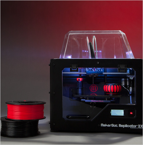
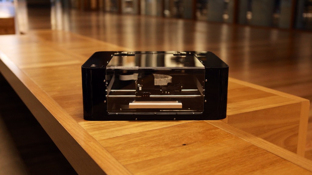
Buy a decent 3d printer <100 micron resolution preferably 50 micron that can print numerous material types, including flexible materials or just resign yourself to find an Objet at a service bureau somewhere and pay $100-200 per print.
We ended up with a Makerbot Replicator 2X (this is the experimental one) I can recommend it, not as accurate as an objet (almost nothing is) but can print numerous different materials, including flexible, wood like material, fluro and conductive ABS and is about 1/10th the price and costs much less to run. Update: We have had a lot of trouble keeping this running smoothly, prints seem to screw up regularly.
We screwed around for a few months designing a fantastic looking watch band and casing and then getting 20 of them built overseas only to find that a, this was never going to be manufacturable and b. it wasn’t at all robust and didn’t allow the sensors sufficient contact, in fact the band material was very soft and didn’t have sufficient stiffness to hold the electronics properly and many aspects didn’t fit correctly despite what looked like a very good design and CAD work and numerous man hours spent between the electrical engineer and the industrial designer (more about that in a minute).
When we started using an Objet 3D printer at a local bureau we very quickly iterated and made numerous major physical design changes in the space of a few weeks and now we have a robust device that looks and feels like a good candidate for field testing but if we had of continued on the previous path we probably would have still been stuck.
While we have salvaged some of the designs there was a month of wasted time in trying to get a physical design to work that was fundamentally flawed.
A week with a 3D printer would have identified this problem must sooner and with a few iterations would have resolved it quickly.
Components, Fabrication & Assembly Leads & Lags
Another reason hardware is hard is that there are long leads and lags in the design and fabrication process.
Every time you have to resign a circuit, its another 7-45 days to redesign, order parts from overseas, etc etch new PCBs and then solder them together and test or have them assembled on an SMD machine.
In software you can change, deploy and test numerous times a day and many companies do this on a continuous deployment basis.
Not so with hardware.
There are a few ways you can mitigate this.
Move to Shenzhen
This is a new title, I only added it this morning after visiting Shenzhen last month. Shenzhen is the hardware capital of the world, prototypes can happen a lot faster here than in other parts of the world.

Be warned its not all smooth sailing, you should be concerned about cultural and communication issues, about theft of your design by suppliers, vendors who are not certified (RoHS, CE etc) being given crap product or not what you agreed.
However after you see the ready availability of mechanical and electrical components in their wholesale trading markets you will understand how this can speed up the prototyping process, we have written a few stories about our visits to Shenzhen here.
So I advise you to get on a plane and spend a month there, I believe it will save you 3-6 months time in the Western world.
Important note concerning buying electronics components in China. You need to be clear what you are buying, processors or genuine brand name items may be counterfeit or recycled. There might be questions over their certifications or compliance. Caveat Emptor.
Ordering Components & Idle Time
Order more components than you need and ship them express. Changing your layout for your Website or App is reasonably trivial and mostly can be done with minor code changes, rarely a complete rewrite.
With hardware you may be discarding your components and logical design and completely rebuilding boards.
When you change your hardware design frequently as you learn and improve your implementation it might seem you are burning through components and wasting money, but this pales in comparison to the opportunity cost of having your engineers idle if you have to wait for overseas component shipments.
We had a few weeks of very slow progress waiting for equipment to arrive that might have been improved with earlier ordering and ordering more than the design called for.
Its tempting to think this is wasteful(I am a tight arse and it grates on me), but in my experience we might be talking about $100-200 in parts but a wasted day for an engineer costs -/+$500 and it’s easy to lose 4-5 days when waiting for overseas shipments.
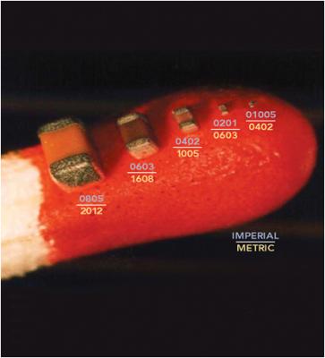
Inevitably you will also break or waste components, if you have ever had to go searching for a 0201 resistor (smaller than I can see with my glasses), that has jumped out of your tweezers you will understand.
You need to provision for wastage.
The lesson here is order as early as you can, pay the extra $50 for express shipment and order 2-3 times as many as you think you will need, arguably buying a huge starter pack of standard and SMD components is a good investment as well.
Alternative Suppliers & Components
There may be alternative suitable components that suit your design and other suppliers who can supply it both locally and from overseas, sometimes an alternative might require an alternative board designs (this could be an issue with FDA approved devices) but if you actually manage to hit the big time and the orders are flowing and you can’t get the original components moving to an alternative design is better than not being able to supply.
These are the most popular, some have Asia Pacific Offices as well as US
- Avnet
- RSOnline
- Element14
- Digikey
You should assess if the components are going to be able to be supplied with consistency. We have noticed in some cases large companies who have fantastic looking processors but they are very difficult to get samples for testing. They often don’t deal directly with the normal components supply chain (Mouser, Digikey, Element14, RSOnline, Avnet) and want to know your forecasts and when you want them before they will provide. (It took me more than 2 months to get a datasheet off one of the big guys and I work for a $6 billion investment fund, 8 months later I still don’t have a sample)
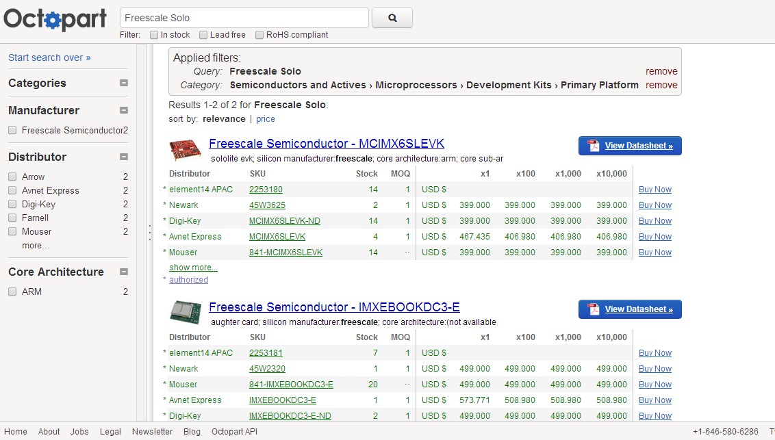
One of the best sites to plug your Bill of Materials into is Octopart.com you can detail all the parts you need and they will display a list of each distributor who holds that part and more importantly will give you the ability to predict costs at volume but allowing you to find alternative suppliers and work out price breaks.
PCB – Make your own or outsource?
Australia like many non manufacturing countries doesn’t have much of a PCB/Electronics manufacturing industry so you can’t just duck down the road and get an updated PCB design fabricated as most of the work is sent offshore.
Initially we started off with basic single layer boards which is easy and fast, later we were building two layer Flexible film circuits using a flexible kapstan copper film and we couldn’t even locate the material locally, it had to be shipped in from overseas.
All the companies who claimed to be able to do this were shipping the work to China with a 2-3 week turn-around time. We couldn’t afford that downtime so initially we decided to make them locally by hand.
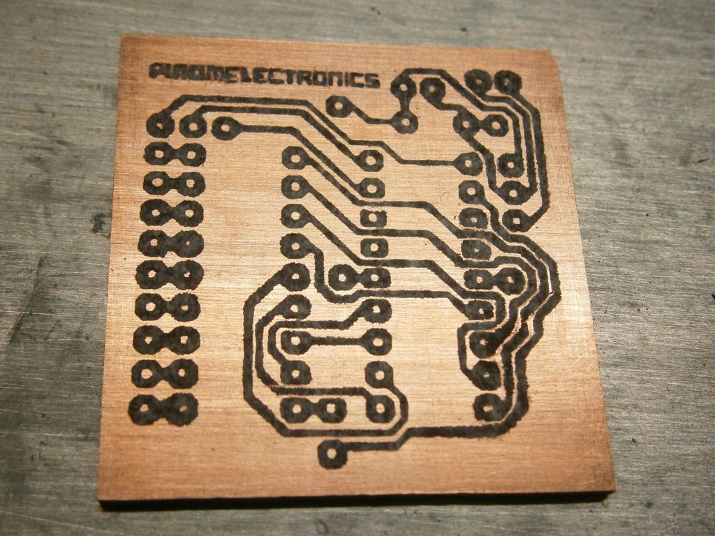
There are a stack of good tutorials on how to do this on Instructables.com but if you want to save time, go straight for the 600dpi laser printing in conjunction with glossy paper and an Iron, having tried a Sandwich press, a laminator and various transfer materials this is what worked best for us.
Making our own was the right decision initially, it gave us a lot of flexibility and we could turn them round in a few hours but what we found though as our circuits got more complex and much smaller, hand fabrication was not very efficient especially the toner transfer aspect was difficult to get right on the very fine traces and we would end up having to to do minor reworks on every board we made.
As our requirements called for smaller designs with higher density and the functionality of the designs was proved it made sense to move to multilevel boards and send this to a prototyping company with the correct equipment.
The lesson is that initially speed and iteration is more important than precision and complexity but as your prototype progresses closer to production complexity increases, you need to go multilayer and speed slows.
Update: Found some locally who can turn these round in 7 days.
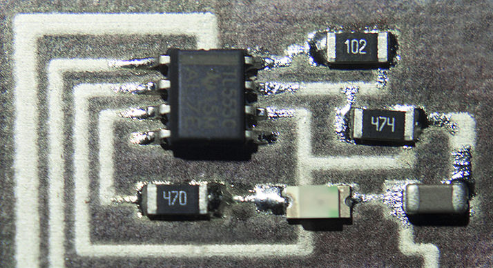
Surface Mount Designs.
We had to breadboard circuits initially, however as many of the sub component designs were available as reference designs from the chip manufacturer, which means you waste a stack of time testing buying through hole components and breadboarding what is a known design and then you have to build a surface mounted version
In hindsight now we are far more comfortable with the process I would suggest that you start with SMD components wherever possible.
Hand soldering SMD components is fiddly and can lead to suboptimal results however most of you probably think its not possible to do SMD without a specialised oven. (they are actually pretty cheap approx $250 SMD Oven on Ebay)

Well you have to ask yourself what would MacGyver do?
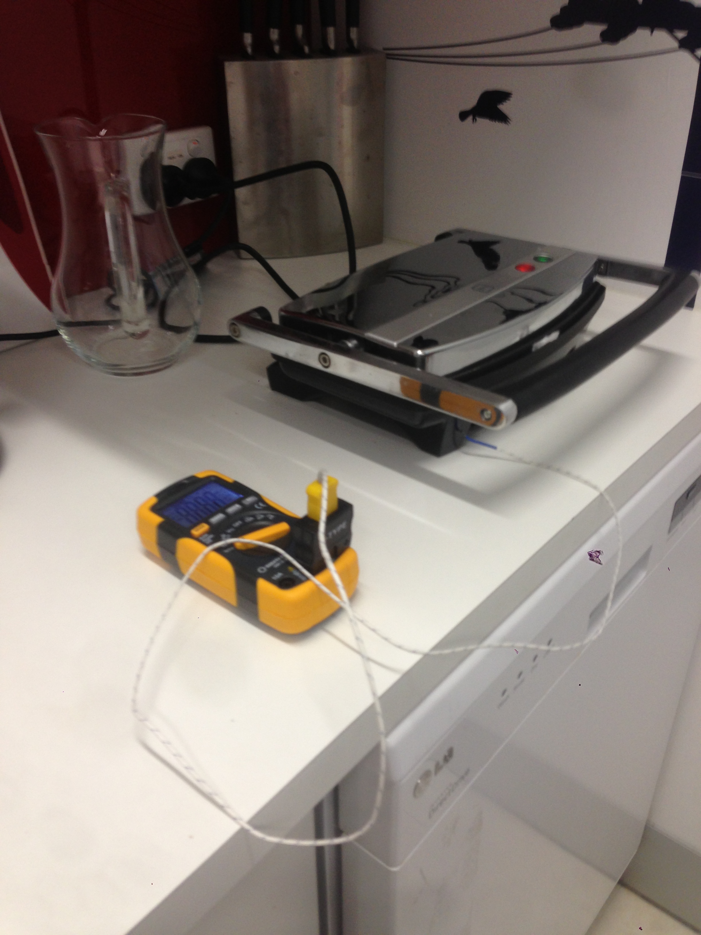
You might be thinking you can’t solder SMD on your bench at home, well here is a trick that has worked very well for us. Its a $20 sandwich toaster and a temperature probe from a $15 Multimeter. Check the SMD soldering requirements for your paste, run the sandwich toaster up to temperature (they normally cook above the required solder temperature) and then check the temperature output on the Multimeter (or you can actually see the solder melt on some of the more obvious components, you can watch it as it happens across the board almost simultaneously).
WARNING: Clearly you cant reuse the sandwich toaster for food, just buy one for this job, they are cheap. Also you can get soldering stations for <$200 which have a reflow hot air gun which might work for some designs.
Reflow SMD soldering saves hours of very difficult hand soldering and is produces a far better result than you can manage with a solding iron.
Originally we did everything on a breadboard using through-mount components

as this was the commonly accepted way of doing things, but it presents a problem.
You need to use normal components through mounting but none of the cool new chips you will want use is going to be through mount, no one makes devices like this anymore, so you will be using SMD components sooner than later.

In hindsight and going forward we will start all new designs with SMD components.
SMD components are so small that if you start to get to any level of complexity you will need to get a PCBA Assembly provider or your own pick and place machine (I think if you are doing any more than 5 assembled boards a year with anymore than 20 per run this will probably pay for itself very quickly in saved time and heartache)
Getting to Production.
We are almost at the point were we are trying to build boards that are production ready.
Different fabrication companies have different design rules about what you can make in their plant and how boards have to be laid out in order to manufacture them.
Most companies have design guides but these are usually only given out once you have established contact or a relationship with them.
Here are a few PCB design resources I found
- http://electronicdesign.com/embedded/engineer-s-guide-high-quality-pcb-desig
- http://www.eurocircuits.com/index.php/technology-guidelines/pcb-design-guidelines
- http://www.altronmfg.com/files/Board%20Design%20Guidelines%202003%20Rev-A.pdf
- http://www.advancedmsinc.com/guidelines.htm
http://www.youtube.com/watch?v=VXE_dh38HjU
http://www.youtube.com/watch?v=Uemr8xaxcw0&feature=share&list=PL3C5D963B695411B6&index=23
Each company will be different so check the design you want to build can be built by your supplier.
The biggest issue is around size of components. If you are designing with 0201 size some assemblers may not be able to handle them, just depends on their machines.
Also there are a few players trying to disrupt the electronics prototype and production process by helping you to design your PCB and then either providing prototype boards or in the case of Circuithub.com turning it into a production version with enough volume to satisfy most new product launches and Kickstarter projects.
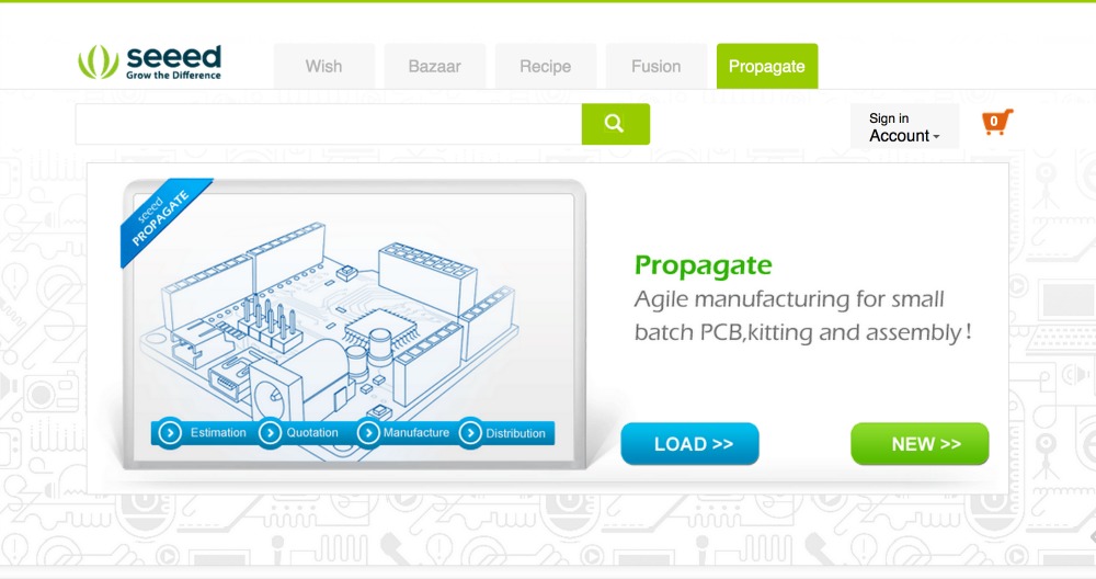
- SeeedStudio has a great prototyping service called Propagate
- https://circuithub.com/
- http://www.123dapp.com/circuits
If you don’t have all the equipment don’t let this get in the way have a look at
- http://www.100kgarages.com/ where “Fabbers” detail the machines and capabilities that they have available for hire.
- http://www.techshop.ws/index.html
- https://www.ponoko.com/
Be unreasonable and always question objections
When one of your team or an interested party tells you something can’t be done you must question it, in my experience its usually the start of a great step forward or an insight.
By insisting on people finding a way to do things they believe are impossible you almost always take steps forward. Sometimes big steps. Sometimes you end up with egg on your face as well but thats ok.
You don’t have to know how to do ir, you just have to know it can be done.
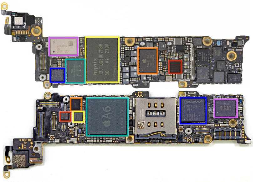
When engineers told me they couldn’t squeeze anymore chips onto the admittedly tiny motherboard for the smart watch, I asked them to look at the Apple 5S teardown photo below.
Its challenging however there is hardly a wasted space on these boards, the designers are elegant in their space efficiency.
Its easy to say well they are Apple you expect this, my answer is me too :).
Tools & Equipment
You either find a great Hackerspace (worldwide list of hackerspaces) that has all the equipment or you are going to buy this within the next few months, better to flex the plastic and get it done.
- Computer Controlled Soldering Station with Hot Air Gun (dont just buy the basic one, you will end up buying the good one later) $100-200
- 3d Printer – Something that can do more than PLA, ie ABS, Flexible, different textures etc and preferably two heads (Makerbot 2X or Hyrel both good but expensive) $2000-5000
- 6 pack of pliers of various shapes and sizes $20
- Component Drawers to keep all your tiny bits $10
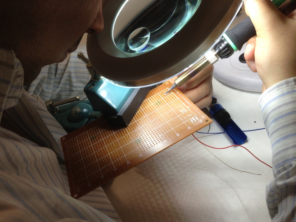
- Magnifying Glass with LED lighting ring $50
- 200x Magnifying glass with USB connection to your PC $100
- Dremel with stand and all the attachments. $150
- Reflow Oven or Rework Station $250
- Wire Strippers $10
- Mini Vice, 3rd hand/Jewellers Vice $20
- Soldering Station Exhaust Fan with filter $50
- Safety kit, masks, eyes, ears, skin $100
- Multimeter $20
- Signal Analyser (might be better to rent)
- Development Kits for the Microcontroller you are working with $100-300
Wish List
- Pick and Place Machine $5000-7000 (make sure they can do the component size you need) I know this is a lot of money however if you can turn around prototypes in 2-4 days not 2-4 weeks you will pay this back extremely quickly and there is a major opportunity cost to slow prototyping.
- Circuit Board Printer like the Cartesian Argentum
 $2000-2500

Move Fast and Make Things
Instead of theorizing and pontificating about if a certain design will work better or solve a problem get cracking and make it, nothing solves an argument like a working device or not.
What are you working on?
Our readers love to hear about new hardware startups and hobbyist projects.
Leave me a message in the attached form about your product and I will write up a story about it
[contact-form subject=’Startup88 – Feedback Form What are you working on?’][contact-field label=’Name’ type=’name’ required=’1’/][contact-field label=’Email’ type=’email’ required=’1’/][contact-field label=’Website’ type=’url’/][contact-field label=’What are you working on?’ type=’textarea’ required=’1’/][/contact-form]
Pitch your Startup, App or Hardware or post a Startup Event or Startup Job